Materials Characterisation
Material characterisation is critical in the production of high quality semiconductor epi wafers which is why Advanced Epi offers a huge range of techniques which generally breakdown into the following categories:
- Non-contact & Non-destructive: Optical inspection, FTIR, XRD
- Non-destructive: 4-point probe, stylus profilometry, AFM,
- Destructive: X-TEM, Hall-effect measurements
Various complimentary techniques are often used to calibrate growth processes for customers' requirements. Almost all of the techniques we offer are "in-house" with a fast turn-around ensuring that calibration and characterisation does not hold up wafer production.
Characterisation Services
Advanced Epi can also offer characterisation services separately from epi wafer growth and we are happy to characterise samples sent to us. For more information on the range of techniques we offer please contact us.

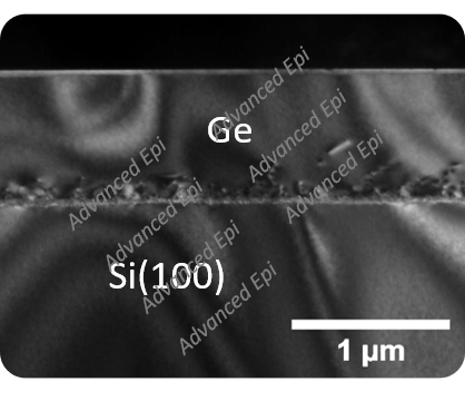
X-TEM micrograph of a Ge epilayer grown on Si(100) substrate
Cross-Sectional TEM
X-TEM enables us to look at the crystal structure of a semiconductor and measure and epilayer's thickness, crystallinity and defects. Sample preparation is critical for X-TEM as the sample must be thin enough for electrons to pass through the sample with minimal interaction. Diffraction imaging is able to distinguish between mono-crystalline, poly and amorphous materials and ensure that epilayers follow the sample crystal orientation of the substrate. Higher magnifications allow us to directly observe the lattice structure of a crystal and identify defect types, formation and annihilation.
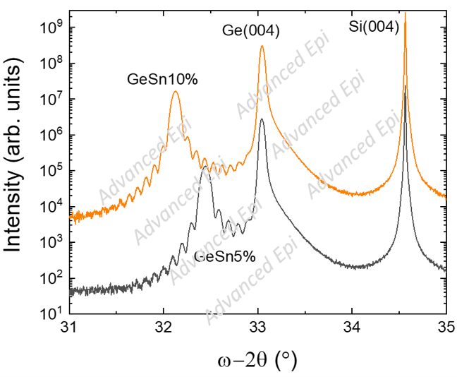
X-ray Diffraction
XRD is the go-to technique for assessing the quality of heteroepitaxially grown crystals. Various scans can be measured including: ω-2θ coupled scans, rocking curves, 2θ-scans, pole figures, reciprocal space maps (RSMs) and more. Various parameters can be extracted from measuring samples by XRD such as crystallinity, lattice constant, composition, strain state and defect types.

XRD ω-2θ coupled scan of a GeSn/Ge/Si(100) heterostructure

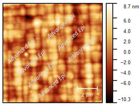
AFM scan of a relaxed epilayer showing cross-hatching.
Atomic Force Microscopy
AFM is a non-destructive technique that measures the surface morphology of an epilayer. The critical parameter extracted by AFM is the RMS-roughness which is a measure of how smooth a layer is. Various properties of a film can impact its roughness such as crystallinity, defect density, types of defects and strain state.
