Si/Ge Quantum Wells
- Quantum Well structures are formed by manipulating the strain and bandgap of semiconductor materials.
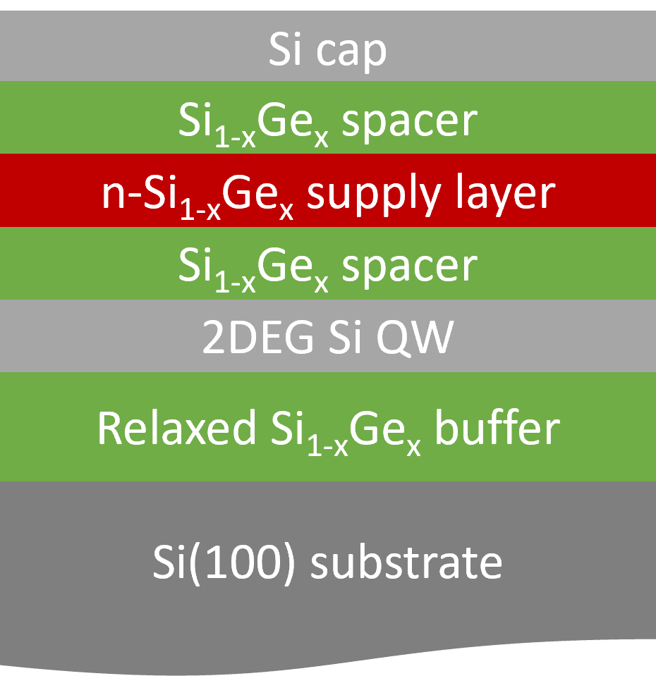
- 2-dimensional electron gas (2DEG) structures can be formed in a tensile strained silicon channel grown on relaxed SiGe.
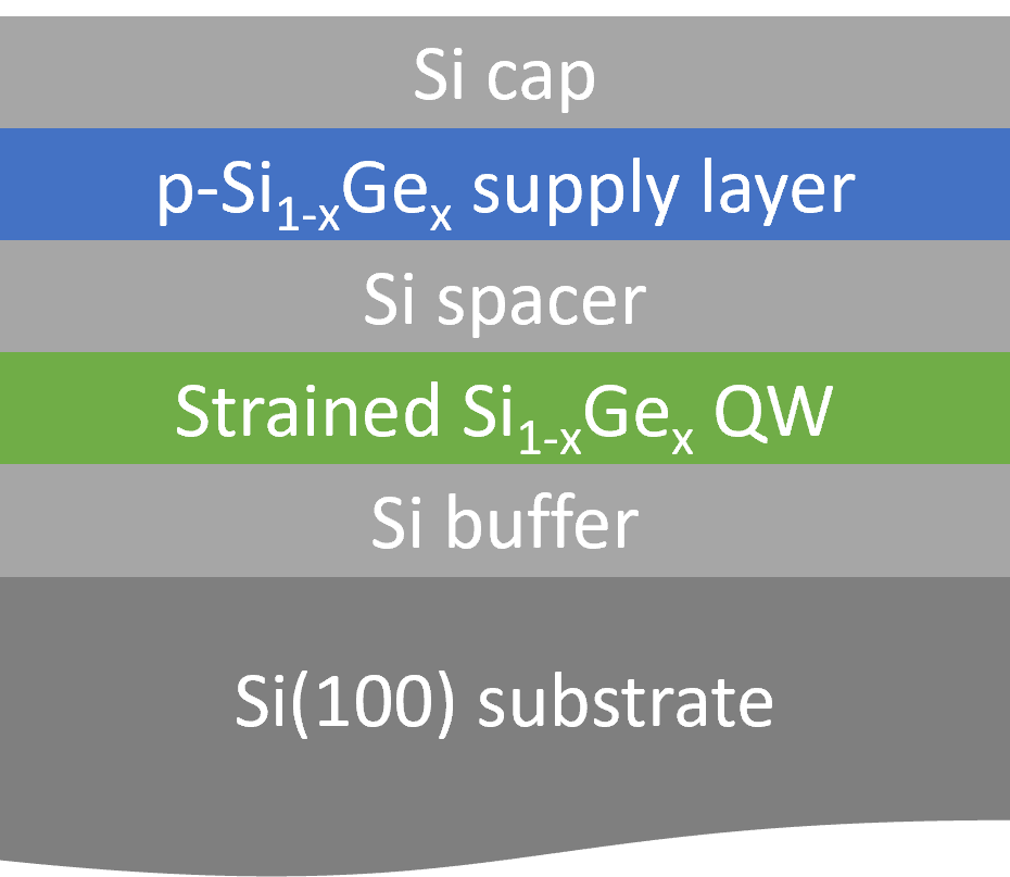
- 2-dimensional hole gas (2DHG) structures can be formed in a compressively strained germanium channel grown on relaxed SiGe or a compressively strained SiGe channel grown on silicon.
- Both structures offer high levels of carrier mobility due to various effects such as modulation doping, strain and carrier confinement.
- Quantum Well structures have various applications where high mobilities are required such as in CMOS, spintronics or terahertz detectors.
2DEG/2DHG Growth
- Advanced Epi can develop and grow Si, SiGe or Ge Quantum Well structures on wafer diameters up to 200mm.
- In depth calibration of each epilayer thickness, strain state, crystal quality and doping is used to optimise the carrier mobility for low temperature or room temperature application.
Heterostructures

Left - Typical silicon Quantum Well (2DEG) heterostructure
Right - Typical SiGe Quantum Well (2DHG) heterostructure

Quantum Wells are complex device structures with various parameters which will all affect the final device operation. If you already have an epilayer stack design we can offer guidance towards successful devices, however, optimisation of 2DEG or 2DHG devices is often iterative and may require several runs to perfect. Please contact us to discuss your requirement with us.
