Device Fabrication
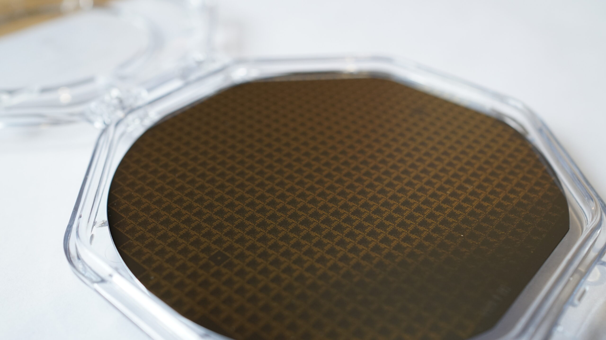
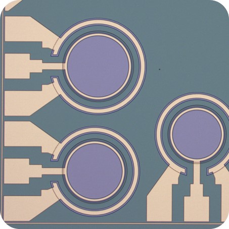
Advanced Epi offers device fabrication services for prototyping, small batch production or extracting electrical properties of epilayers. Various in-house processes allow us to rapidly design and fabricate device structures. Thanks to our maskless laser writer we can pattern your digital mask files directly onto chips or wafers or if you already have a defined mask design we can pattern entire wafers using our mask aligners.


Device Fabrication Techniques
Lithography - laser writer, UV mask aligners
Metal Deposition - e-beam evaporator, sputtering
Etching - Wet etching, RIE-ICP
Oxidation - PE-CVD, TEOS, thermal
Most of our processes are capable to handling chips, 100mm and 150mm wafer diameters.
Electrical Characterisation Techniques
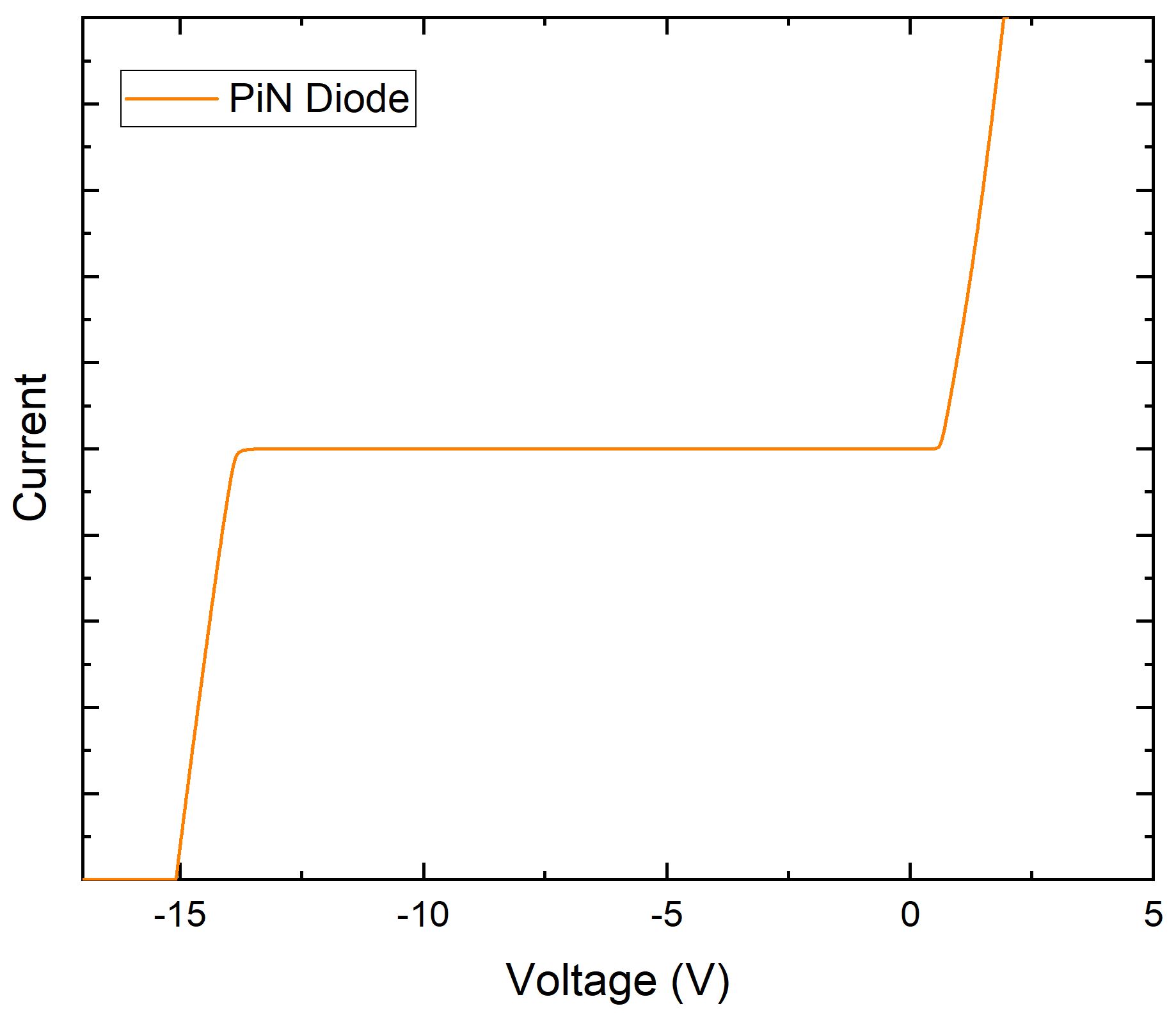
In-house characterisation techniques allow us to extract vital electrical data from your devices as a complete package solution.
I-V (77K to 800K)
C-V (77K to 300K)
Hall Effect (15K to 300K)

