Material Characterisation
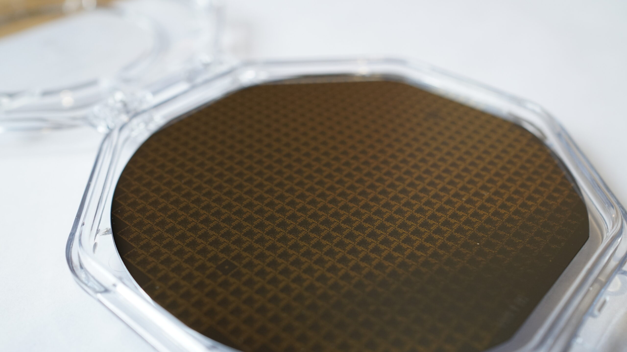
Advanced Epi can provide data of grown epi wafers utilising a range of characterisation techniques. Non-destructive techniques which can be carried out at wafer scale include AFM surface roughness, FTIR thickness uniformity and wafer bow mapping. More in depth characterisation can be performed using SEM, TEM, Raman techniques as well as electrical characterisation including temperature dependent Hall effect and resistivity measurements.
Device Fabrication
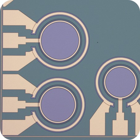
All grown epi wafers can be processed into prototype devices using our in-house fabrication facilities, which include:
- Lithography - Mask aligners and Maskless Laser Writer
- Etching - RIE-ICP dry etch and various wet etchant solutions
- Deposition - Metal and oxide deposition by evaporation or sputtering
- Packaging - Wire bonding (Au or Al)
- Test - Variable temperature probe stations (I-V/C-V), Cryogenic Hall effect
Process Development
Advanced Epi works closely with customers to provide a truly bespoke epitaxial service and often develops processes specific to each applications and set of requirements. All of our epitaxial growth is carried within industry standard cold-wall CVD reactors which facilitates seamless integration of our processes into other manufacturing lines.
A wide range of processes beyond epitaxy can also be developed in-house to facilitate your development projects. If you are looking to develop a new technology or expand into new markets we can offer unique service to facilitate and accelerate development without impacting on your own vital internal processes. For more information about the services we offer and how we can assist your own projects please contact us.


