Germanium Tin (GeSn)
- Germanium Tin (GeSn) is an alloy between pure Ge and Sn
- Adding Sn to the Ge lattice transitions pure Ge into a direct bandgap semiconductor and offers the ability to control the bandgap itself
- Applications include: IR LEDs, LASERs and detectors for various communication applications with the ability to tune photodiode wavelength between 1550-3000nm
- Typical device structures include pure GeSn or hybrid Ge/GeSn PiN photodiodes as well as GeSn/Ge/Si APDs
- Advanced Epi is one of the only global providers of GeSn epitaxy on (100, 150 and 200mm) diameter wafers offering significant cost savings over III-V material technologies and a great contender for new low-cost LIDAR detectors
Germanium Tin Growth
- Advanced Epi can grow high quality GeSn (strained or relaxed) up to ~13% Sn content
- Advanced Epi grow GeSn alloys on relaxed Ge buffers grown on Si(100) substrates with buffer thicknesses typically 600-1000nm
- GeSn Epilayers can be grown on 100, 150 and 200mm diameter substrates
- Electrically active doping is possible with both n-type (P) and p-type (B) dopants
Material Characterisation

Cross sectional schematic for GeSn epilayers grown on Ge buffers (virtual substrates).

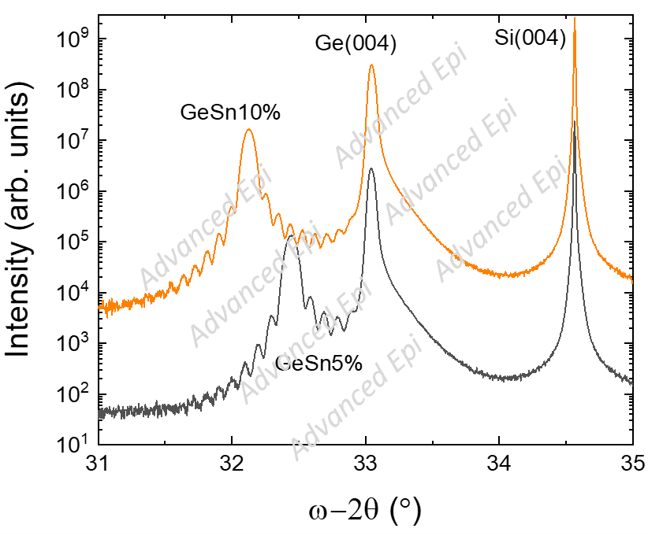
X-ray diffraction (XRD) coupled scans of fully strained GeSn epilayers of 5% and 10% Sn composition.

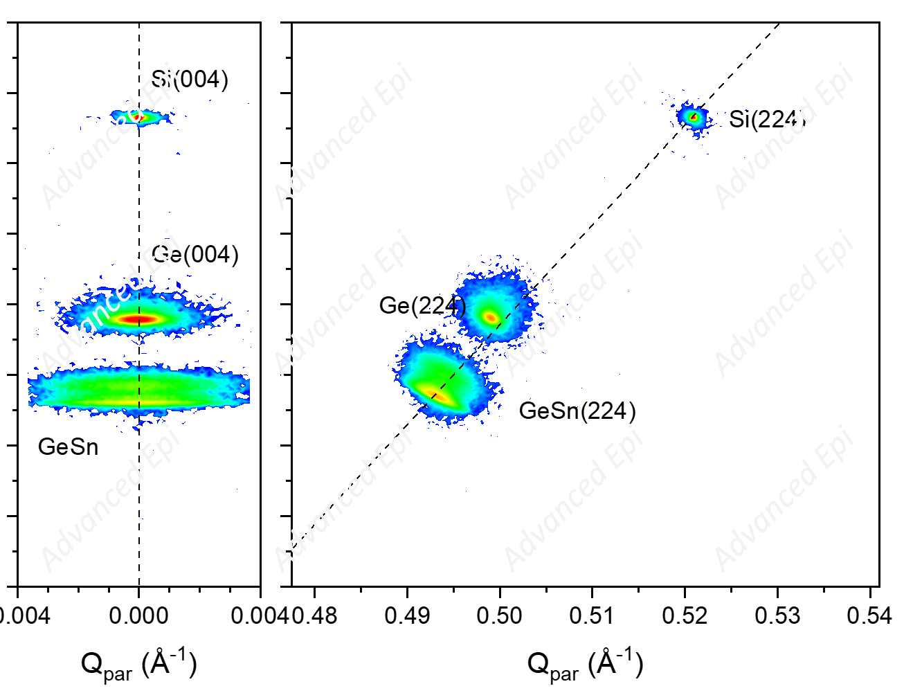
Reciprocal Space Map (RSM) of relaxed GeSn epilayer suitable for photonic applications.

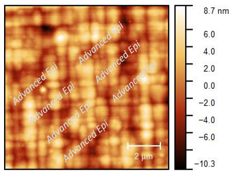
The surface roughness of GeSn epilayers tends to increase with Sn content, thickness and relaxation although films with RMS roughness <2nm are possible.

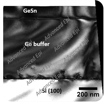
Cross-sectional TEM image showing high quality GeSn epilayer grown on a relaxed Ge buffer.
