Germanium (Ge)
- Germanium is a semiconductor with a bandgap of 0.67eV which is narrower than pure silicon
- Germanium can also be alloyed with silicon in any composition enabling complex strain engineering possibilities which can enhance properties of the semiconductor
- Germanium and silicon germanium (SiGe) alloys are used in various high-speed integrated circuits, wireless communication and photonic applications including PiN and APD structures for various IR sensing and LIDAR applications
Germanium Growth
- Advanced Epi grow germanium directly on silicon substrates (100, 150 and 200mm).
- While germanium substrates are available, the added cost, poor surface finishing and susceptibility to contamination make homoepitaxial growth of Ge challenging, although Advanced Epi can still offer this service
- Growth on Si substrates introduces dislocations due to lattice mismatch but through careful growth processes these can be minimised and controlled.
Material Characterisation

Cross-sectional schematic of Ge epi wafer. Epilayers are typically grown up to ~2µm thick.


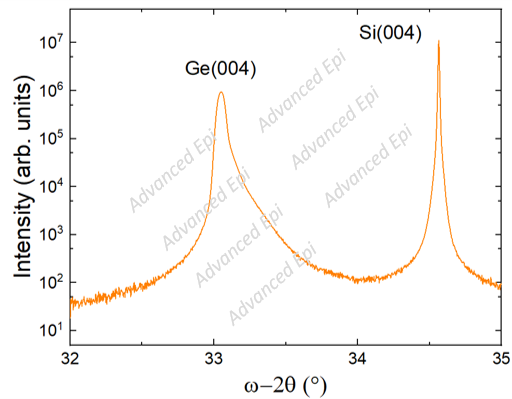
X-ray diffraction (XRD) coupled scan showing a monocrystalline Ge epilayer grown directly on a Si(100) substrate
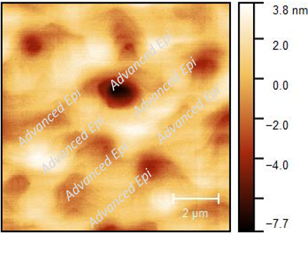
Surface morphology of Ge epilayers tends to improve with increasing epilayer thickness and an RMS roughness of 1-2nm are possible with 1µm thick Ge films.
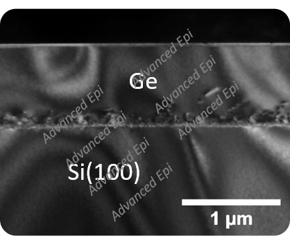
Cross-sectional TEM confirms high quality Ge epilayers with uniform thickness and low dislocation densities.
