Group IV Epitaxy
Advanced Epi offers a wide range of epitaxial materials including silicon, germanium and various alloys. We hold a stock of epi wafers for immediate dispatch that are available in low quantities for small scale R&D and evaluation, details of which can be found on our online store.
A non-exhaustive list of materials we have the capability to grow and their typical applications is given below:

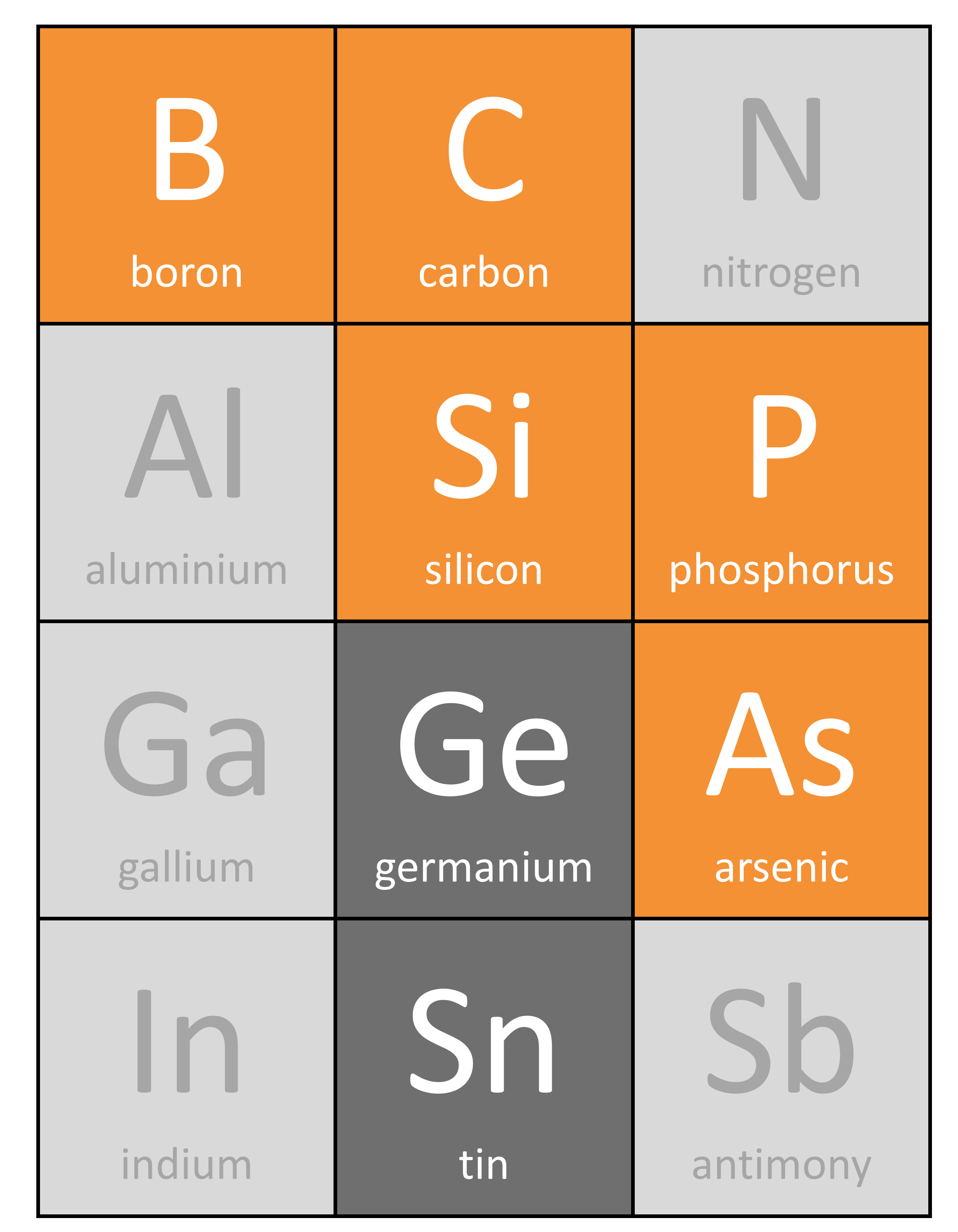
Silicon, Si1-xBx and Si1-xCx Alloys
Silicon can be grown up to 10's of microns and can be doped with B (p-type), P or As (n-type) during epitaxy. Advanced Epi specialise in novel Si growth processes such as selective epitaxy or growth on non-standard substrates.
Alloys including silicon boron and silicon carbon with % levels of B or C incorporated in the lattice can offer exciting applications in strain engineering and lowering contact resistance.

Cubic Silicon Carbide
3C-SiC is grown using Advanced Epi's novel low temperature process within standard Si-based cold-walled CVD reactors. High crystal quality, low surface roughness and minimal wafer bow is achieved.
3C-SiC epilayers can be grown from 10's nm to to ~1micron on substrate diameters up to 200mm with high levels of electrically active n-type dopants. MORE INFORMATION

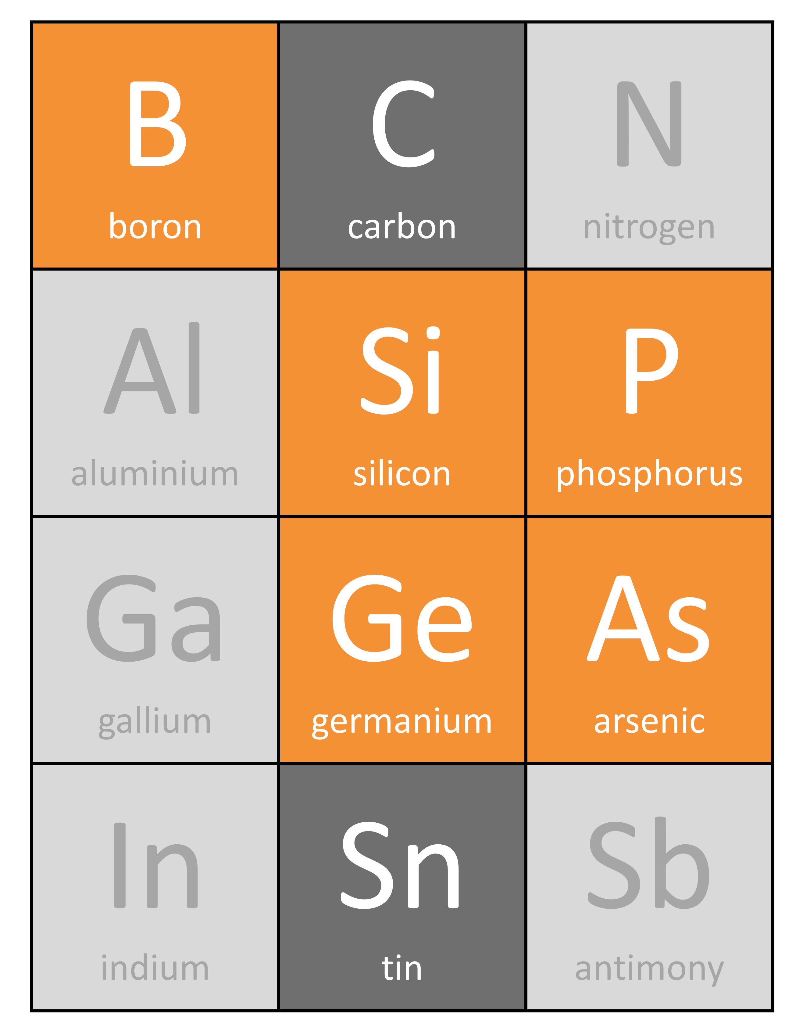
Germanium and SiGe Alloys
High quality germanium epilayers can be grown on Si substrates offering very low defect density virtual substrates. Typical thickness of buffers ranges from 200nm up to ~1um although thinner / thicker Ge may be available on request. MORE INFORMATION
Silicon Germanium (SiGe) alloys can be grown directly on Si substrates or on Ge virtual substrates. Pseudomorphic SiGe can be grown fully strained to the Si or Ge substrates and thicker strain relaxed buffer layers are also available. MORE INFORMATION

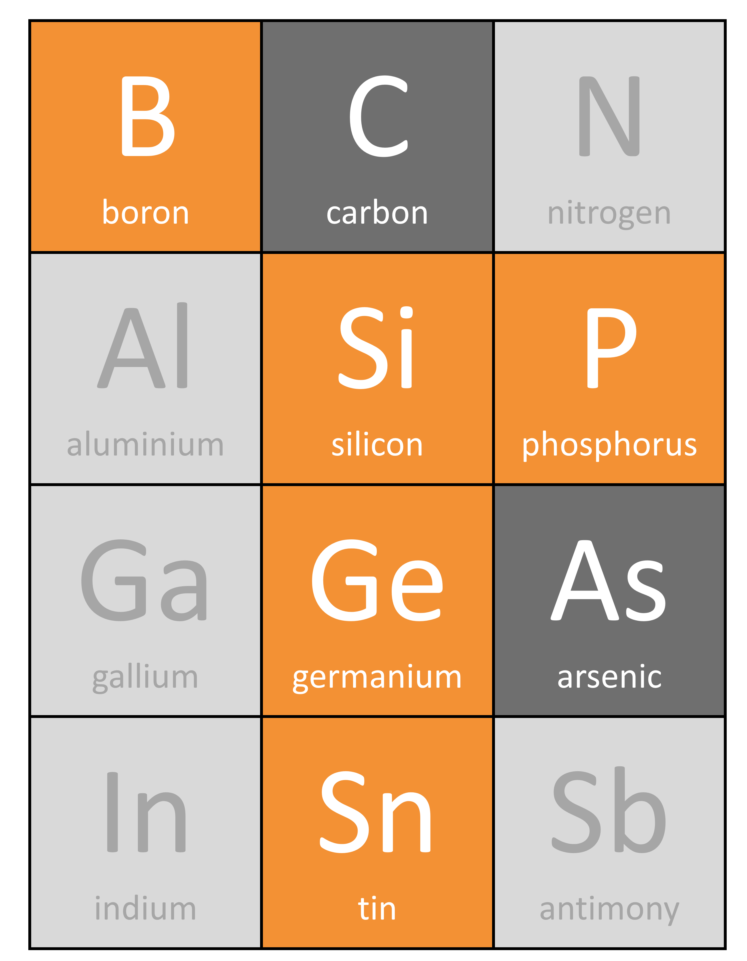
Germanium Tin Alloys
GeSn is an exciting new semiconductor material which offers bandgap manipulation promising the first direct bandgap Group IV semiconductor for IR photonic applications. While growth of GeSn is still in the experimental phase, Advanced Epi can offer strained and relaxed epilayers up to ~12% Sn content. MORE INFORMATION
Substrates and Growth Processes
Almost all our epilayers can be grown on (100, 150 and 200mm) diameter substrates.
Advanced Epi holds a wide range of Si substrates in stock, please see the table below for typical parameters.
| Material | Wafer Diameter (mm) | Orientation | Thickness (microns) | Offcut (degrees) | Doping type | Growth Process |
|---|---|---|---|---|---|---|
| Silicon | 100, 150, 200 | (100), (111) | 350-1000 | 0-4 | n-, p-, n+, p+, FZ | Cz, MCz, FZ |
We can also grow almost all of our epilayers on SOI substrates as well as SiO2 patterned substrates for selective epitaxy. We are happy to grow on substrates supplied by customers but may require certificates of conformance to validate cleanliness.
