Group IV epitaxy services tailored to your application
Advanced Epi offers a range of bespoke epitaxy services focusing on the group IV semiconductor materials including silicon, germanium, silicon carbide and their various alloys. In addition to supplying epitaxial materials, we specialise at in-depth material characterisation, device fabrication and process development.
With access to cutting-edge processes and techniques, Advanced Epi is the ideal partner for organisations looking to develop new technologies or expand into new markets. We work very closely with customers to understand their requirements and offer them a truly bespoke service. All of our techniques and processes are standard to the Si-industry offering seamless transfer into your own facility or preferred foundry should your demand exceed our capacity. Please contact us to discuss your project or material requirements.
Group IV epitaxy
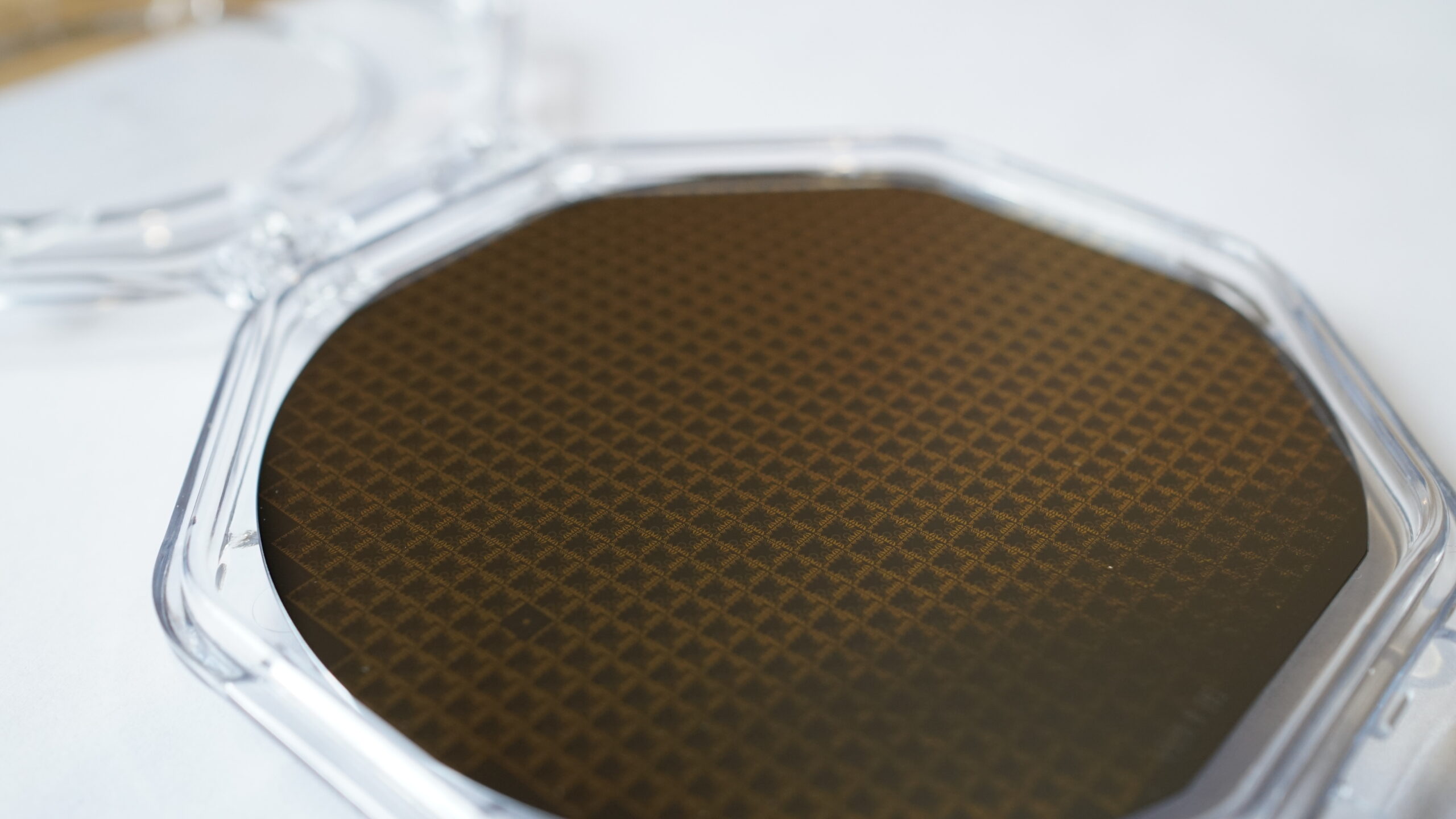
Advanced Epi supplies a wide range of group IV based materials including silicon germanium as well as many alloys such as SiGe, GeSn, SiB and more. Epilayers can be grown on 100, 150 and 200mm Si substrates as well as SOI or patterned substrates for selective epitaxy.
3C-SiC Epitaxy
Advanced Epi's patented process enables the growth of high quality 3C-SiC films on silicon substrates using standard CVD growth processes found in the silicon industry reducing cost, minimising thermal stress and increasing wafer size and volumes.
Device Fabrication
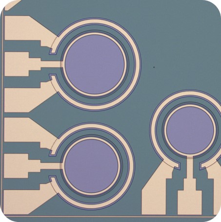
Advanced Epi has in-house device fabrication capabilities which allows us develop entire process chains from epitaxy to device fabrication and testing. The electrical properties of epilayers can be studied in great detail through the fabrication of test devices offering in-depth material calibration.
Characterisation
Advanced Epi can provide a range of material characterisation data on grown epi wafers using a range of destructive and non-destructive techniques including but not limited to FTIR thickness uniformity mapping, AFM surface morphology, X-ray diffraction, SEM, TEM and electrical characterisation.
About us
Advanced Epi is a UK-based company founded in 2015 and offers semiconductor epitaxial materials and services. The company has access to world-leading facilities and semiconductor growth processes, making Advanced Epi the ideal partner for any organisation looking to develop new technologies. Not only can we supply standard epitaxial materials but often work very closely with customers on new experimental projects, offering knowledge and expertise to help develop processes specific to their application and requirements.
Advanced Epi works with organisations of varying forms and sizes from academic institutions, SMEs looking to disrupt the market and multinationals interested in maintaining a competitive edge in their field. We are happy to supply small quantities of wafers for evaluation purposes and can grow with a project, supplying larger batches for high volume production. All of our epitaxial processes are backed up with a wide range of in-depth material characterisation techniques offering precise control of our material properties. For more information on the techniques and processes we offer please click here.


