Silicon Germanium (SiGe)
- Germanium can be alloyed with silicon in any composition enabling complex strain engineering possibilities which can enhance properties of the semiconductor
- Silicon germanium (SiGe) alloys are used in various high-speed integrated circuits, wireless communication and photonic applications
- Advanced Epi offer SiGe epitaxy on 100, 150 and 200mm diameter substrates
Silicon Germanium Growth
- SiGe alloys can be grown at any composition from 0-100% Ge content
- Low Ge content alloys (<50%) are typically grown directly on Si substrates while higher composition Ge alloys (>50%) are grown on relaxed Ge buffers
- SiGe epilayers can be grown fully strained, partially or fully relaxed
- The critical thickness (above which SiGe will usually relax) varies with Ge content which can limit possible thicknesses
Material Characterisation

Left - Cross sectional schematic for SiGe epilayers grown directly on silicon. Right - Cross sectional schematic for SiGe epilayers grown on relaxed Ge buffers (virtual substrates).


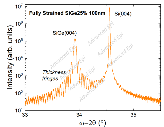
X-ray diffraction (XRD) coupled scan showing a fully strained SiGe25% epilayer grown directly on a Si(100) substrate
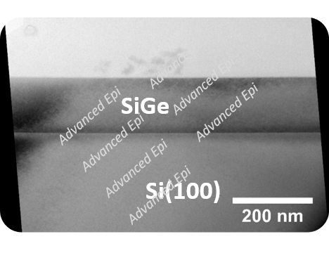
Fully strained SiGe epilayers are typically defect-free retaining a surface morphology similar to that of the silicon substrate.
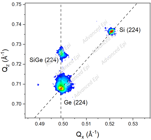
Reciprocal space map (RSM) showing a SiGe70% epilayer fully strained to a relaxed Ge buffer.
