3C-SiC Growth
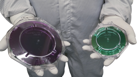
Advanced Epi's process enables the growth of cubic silicon carbide (3C-SiC) on standard silicon (Si) semiconductor wafers at low temperatures, without compromising on quality or growth rate. The key advantages of this process are:
- Reduced thermal stresses
- Compatible with silicon technology
- Low-cost and high volume


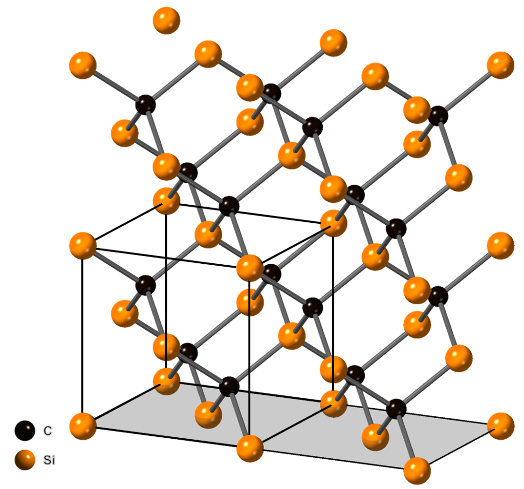
Being a wide bandgap semiconductor, intrinsic 3C-SiC offers high resistance and semi insulating properties.
Very high concentrations of electrically active dopants (p-type or n-type) can be introduced into the 3C-SiC epilayers during epitaxial growth which can help avoid unnecessary ion implantation steps in device fabrication.
Advanced Epi offers 3C-SiC grown on standard (100, 150 and 200mm) Si wafers and can also grown on SOI or patterned substrates for selective epitaxy
3C-SiC Sensors
3C-SiC is a wide bandgap semiconductor capable of operating at very high temperatures and withstanding the effects of corrosive chemicals. These properties make it an ideal material for sensing devices for harsh environments.
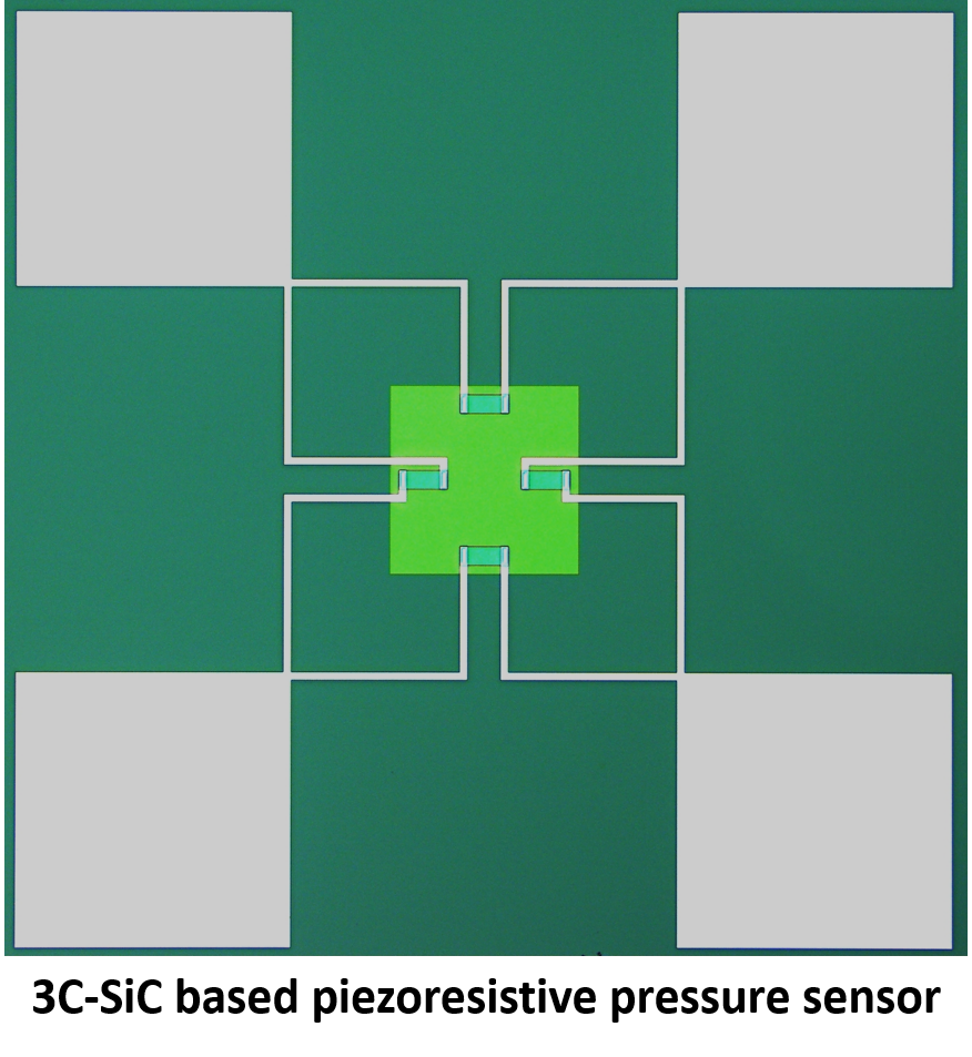
Advanced Epi is working on novel devices based on 3C-SiC that will be able to measure a range of variables including: pressure, temperature, gas flow, magnetic fields, UV light...

Platforms for GaN
3C-SiC is also an ideal template for the growth of gallium nitride (GaN). The crystal structure of 3C-SiC offers a lattice spacing that is only 3.5% mismatched to GaN (compared to 17% for silicon and 14% for sapphire) which means growing GaN on 3C-SiC will result in fewer crystal defects and higher performance devices.

Both hexagonal GaN and cubic GaN can be grown on the SiC/Si template and depends on the starting crystal orientation of the silicon substrate.
- Reduced defect density
- High thermal conductivity
- Block diffusion of materials
The resulting GaN has applications in radio frequency mobile communications, power electronics and LED light emission.
3C-SiC Membranes
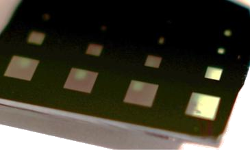
Advanced Epi's 3C-SiC is also suitable for the fabrication of suspended membranes. Material as thin as 25 nm can be suspended through the etching of the underlying Si substrate in standard anisotropic wet etchants.
Membranes can form the basis of 3C-SiC pressure sensing devices, optical windows and sample grids for electron microscopy.

